Recent Blue Posts
 Season of Discovery Hotfixes - 23 April
 Season of Discovery Hotfixes - April 23
 Dragonflight Season 4 Content Update Notes
 Obtained a rare mount? Link the Screenshot!
 MMO-Champion
Ok as the title implied, I'm interested on what the actual functional differences are between a CPU and GPU. I don't mean the difference between a graphics card and a processor, I know that each are seperate and what not. What I am actually interested in is the actual architectural and physical differences between a processing core in say an i5-2500k against the core in a GTX560, how do they perform differently and more importantly... why?!
As far as I can see, they're pretty much the same thing, applied in different ways, and I'm 99% sure that's not correct. Can someone particularly computer savvy fill me in on possibly the most trivial of computer matters?
 Recent Forum Posts
Thread: CPU/ GPU differences.
-
2011-12-22, 10:22 PM #1Deleted
CPU/ GPU differences.
-
2011-12-22, 10:31 PM #2High Overlord

- Join Date
- Apr 2009
- Posts
- 179
Short version:
CPU can do any instruction set and is multipurpose: memory management, calculations, I/O ect ect
GPU is designed for a specific task: Video. With many parallel instructions going on.
A GPU will have more transistors then a CPU but those will run slower then CPU transitors (thats why they are bigger then CPU's, they need more)
That being said, there is a move from letting a GPU just do Video and making it act more like a CPU with Cuda and other CPU like instructions sets.
Best way to view it is to put a Console up against a Computer. While the Console might be slower on paper, its components and inner working make it dedicated for the taks (games) and the Computer is more multitaks and thus will run the same games slower as they will be better optimized for the console.
-
2011-12-22, 10:37 PM #3Stood in the Fire


- Join Date
- Jul 2009
- Location
- The Internet
- Posts
- 406
You have what is called the "Die" or "Architecture" of a CPU and GPU, that is the design, number of cores, the cache ect ect, all these things are physicall parts of a Processing unit. A cpu is designed to handle everyday tasks and making calculations efficiently. Where as a gpu is designed to handle tasks like rendering 3D Design and tasks of that nature more efficiently.
Both the CPU and GPU designs are different, They have Different Die's and architectures. This goes also for a range of different CPU's and GPU's an I7 990 is different from an i7 3960x they have different Die's.
A cpu comprises of up to 8 cores in the consumer market (more for servers/workstations) with a few cores being disabled. i believe the i7 3960x has 8 cores, 2 disabled. GPU's comprise of hundreds of cores.
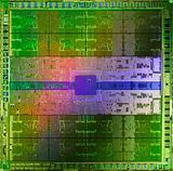
Here are two pictures.
I5 2500 DIE:
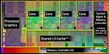
GF100 Die:

-
2011-12-23, 12:48 AM #4Titan
- Join Date
- Apr 2009
- Posts
- 14,326
CPU for a PC computer is very complicated device. It can run few hundred different instructions that range from very simple to very complex, and it's optimized to run those sequentially as computer programs are run sequentially from start to finish. Biggest thing that speeds up CPUs in past five years or so is guessing what instruction comes next based on what came before, and starting to work on that already while waiting for the real instruction to arrive from memory. Originally Posted by StarbuyPWNDyou

GPU on the other hand is very simple device. It knowns only a handful of instructions that are mostly matrix multiplication, and is optimized to do those multiplications really really fast. Because drawing screen can be done in parallel (line at a time or column at a time), normal method for speeding up GPU is adding more and more and more of those simple multiplication units to run in parallel. Modern GPU can have few thousand of those. So if you have 1920x1080 screen, 2000 parallel processors can do whole line all at once instead of going left to right, top to bottom like you'd read text.Never going to log into this garbage forum again as long as calling obvious troll obvious troll is the easiest way to get banned.
Trolling should be.
-
2011-12-23, 05:22 PM #5FuzzeekeeGuest
A CPU is a term for a "general purpose" microprocessor. GPUs are very specialized, they are basically in the high speed ASIC category...
There are many types of processors, NPUs, GPUs, CPUs...Each one is designed for a specific task.
Here are some examples of digital logic with "gates" before I explain more:
CPU: Mostly Serial (General purpose, only good at everything, not good at one thing)
GPU: Mostly Parallel (REALLY good at a particular thing, but lacking broad features)
NPU: Network-processing-unit...A custom ASIC (application specific integrated circuit) usually with a special microprocessor built in, or whatever the manufacturer wants in there...
PLD: Programmable-Logic-Device: FPGA -> Full of multiplexers and SRAM cells for DESIGNING your own GPU, CPU, NPU, whatever you want that uses logic gates...
PLD: ASIC -> VERY VERY expensive, but insanely fast, preferred for fighter jets, phalanx cannons, worthwhile things, etc
PLD: CPLD, FPGA, ASIC/ASSP, etc
The rule is anything that uses logic gates can be simplified to 3 gate types: NOT, OR, AND ...You use boolean algebra to simplify a complex design(which is hilarious because this sounds complicated man, but it's as simple as grade 8 math. You can google this also, and later I will link you to an e-learning site with some of the most popular manufacturers)
Now basically how the companies make these, is they will have expensive simulation software, and things like altium designer. A team of "digital engineers" usually will design in a group for X target, based on cost, time, etc...And there is a design flow which usually has test phases all over it. The simulation software will check your timing and, routing, etc (to make sure you don't have gate switching problems and power estimation issues)...AMD and NVIDIA typically will hand-route most of these devices, but the internal design cycle of those companies isn't known to me, or even important as I just have a "general" digital engineering background...
Once you have your silicon device simulated, you need to do place and route, and set up your board. There are a lot of options for a printed circuit board. FOR a GPU specifically it has its OWN power system on the PCB, and it rises from the motherboard on a PCI-X slot...It's complicated, it's not as simple as some people make it sound.
You can make many types of PCBs, they typically have 4 to 8 layers. There are little "roads" that connect the silicon device to everything and we call these traces...The reason the board can be 8 layers, is because with a complex design, the board can be more efficient, and routing can occur at multiple layers and carry over to different parts....Next we come to the silkscreen which is the "cool looking" writing you can get done, or anything to aid in design...Usually an expensive silkscreen is actually for these MASSIVE machines called pick and place machines which will just smoke down your parts with insane accuracy...You can also choose the solder mask color. ANY color almost with a big OEM...If you guys are reading this I wonder if you remember all those cool purple motherboard PCBs from the 90s. GREEN though is typically the cheapest PCB solder mask, but it DOES NOT mean the thing sucks...
GPU design is done by in house electrical engineers, and once it's done, it will go to a foundry, such as TSMC (taiwan semi-conductor)...That's the biggest name and I picked it because it's the most common and easy to understand for everyone here. There are loads of good foundries, even local ones. Once it gets there, you have to worry about process nodes (how big the gates are going to be on a wafer)...It varies a lot. Each foundry will charge based on the best wafer/node available...Usually when a process node has been around for awhile the yield (how many chips can come out as good, and ones as bad) is very high, because it's always improving...It's often better to design at 65nm then move to say 45nm, if the 45nm one is too new. In fact in a lot of cases the 65nm chip will come out better because the node has improved over time (people are always constantly working on each node because each customer is different)...Plus they charge more for different nodes. There are a lot of good benefits for being at a smaller node. Your power envelope almost always gets slashed in half compared to the old one. No silicon device is made the same, basically they use these chemical reactions to make little gates that look like semi-conductor playdough when viewed up close under a special tool which can see things of such size...When you have low yield, the gates will be more goopy looking and they don't have a good chance of "lining up", and your wafer can only have a few good units on it. It's risky, and usually only the richest companies will go towards that right off the bat...
On PCB design: Anyone can design a PCB, if you WANT to design your own, and you're scared or you don't know what to do, yet you have an idea. You should contact a company for what we call a "turnkey" solution. Where they design the entire thing for you. Expensive, but it's there...
I really hope you have fun, happy holidays man
Take a look at this: http://www.altera.com/education/training/trn-index.jsp
Lots of free courses to get you started. I personally prefer VHDL for my logic gate design. It's a C-like language for making your own CPU or whatever you want....People have done all kinds of cool things, from remaking old cray supercomputers from the 70s, to an openSPARC 8 core CPU...There's a lot of boards you can get. An entry level 80$ board is just fine, but a $500 board is good enough for an advanced student/professor who is researching...

 Reply With Quote